Cambridge Audio Azur 640R (7.1 Speaker Amplifier)
Introduction
From the mid 2000s, this 15kg (33lbs) behemoth is a 7.1 surround sound speaker amplifier, able to power each of the seven speaker channels at 100 watts rms (into 8Ω), or just two channels at 120 watts rms each, with a maximum power draw of 1400 watts. This is the most powerful amplifier (for the price) I could find second-hand on eBay, and has other features including HDMI switching, and capabilities for multi-room connections.
Ports, Buttons & Knobs
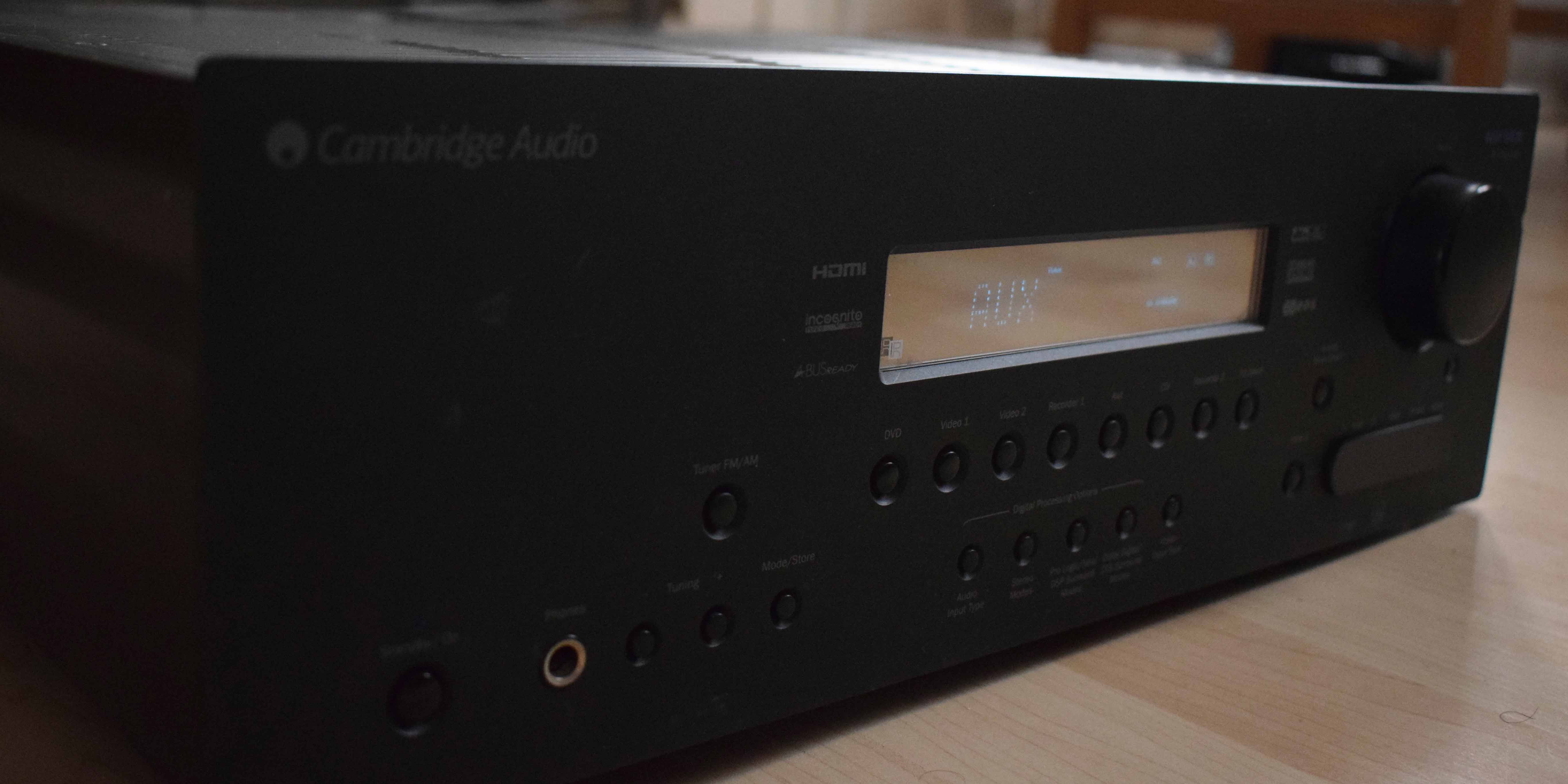
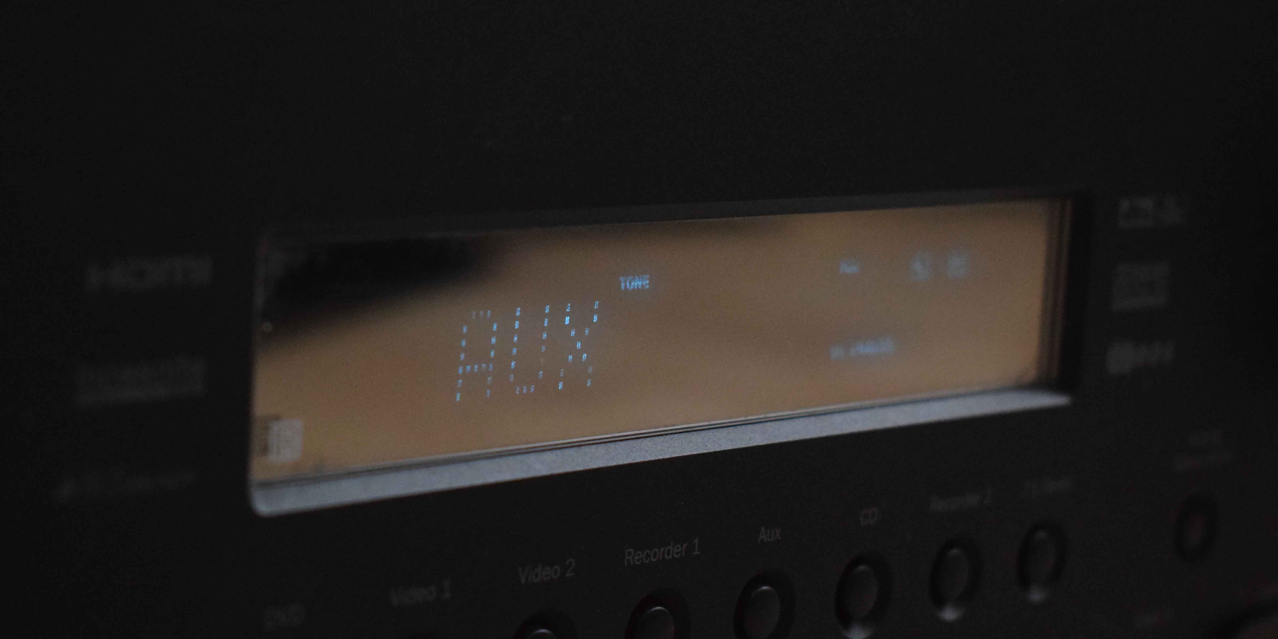
Before disassembly, lets just take a look at the physical features of the device. Starting from the front, it features a blue-tinted Vacuum Fluorescent Display (VFD) - which I didn't even realise until cleaning it as the display lens was entirely stained with dust - as well as a series of buttons for power, inputs, AM/FM tuner, digital sound processing, and speaker modes. There's a mute button next to the volume knob; a 6.35mm headphone port; and a set of audio/video ports for "Video 3" hidden by a plastic cover. All of this is mounted to a thick metal plate that alone is a fairly significant weight.
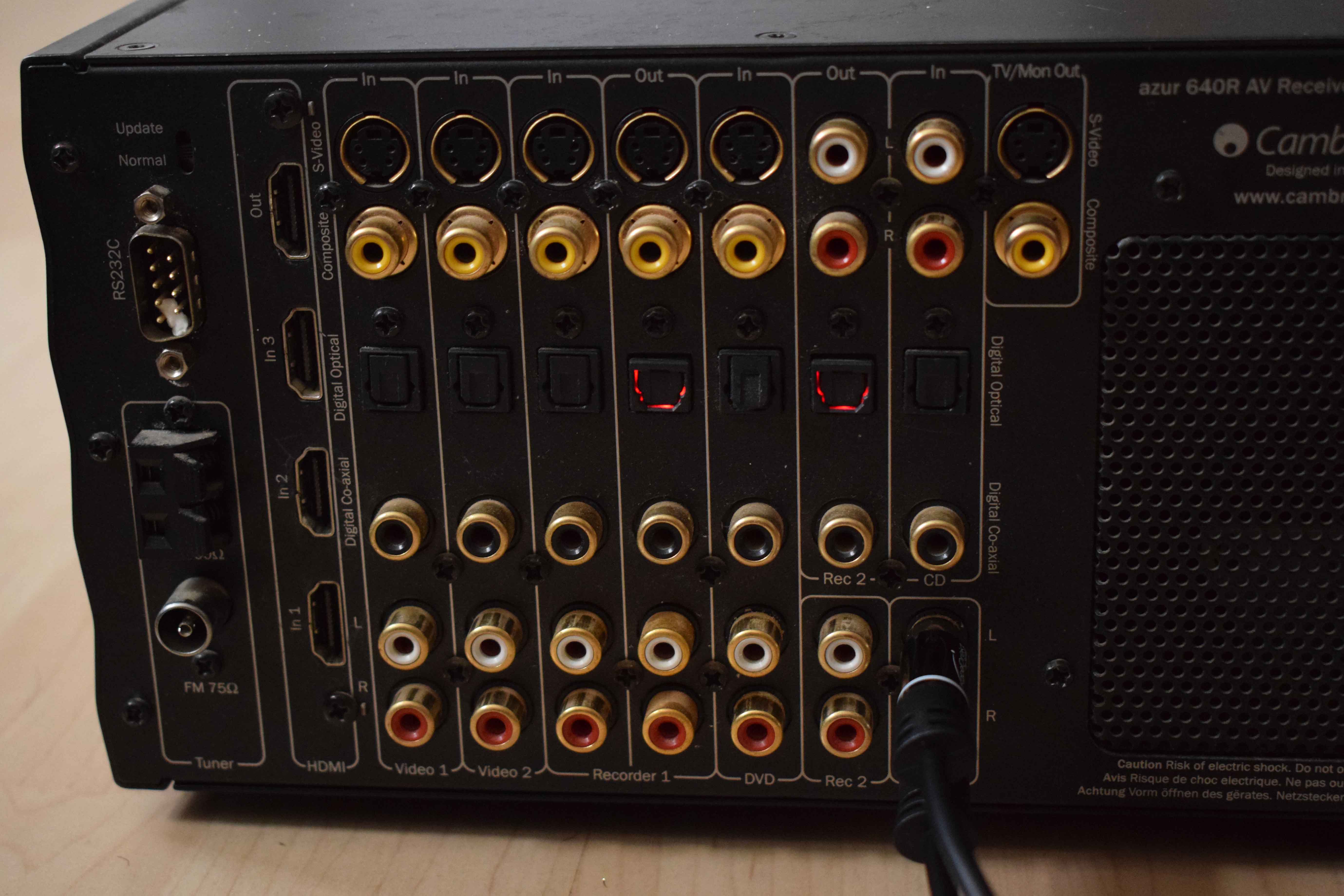
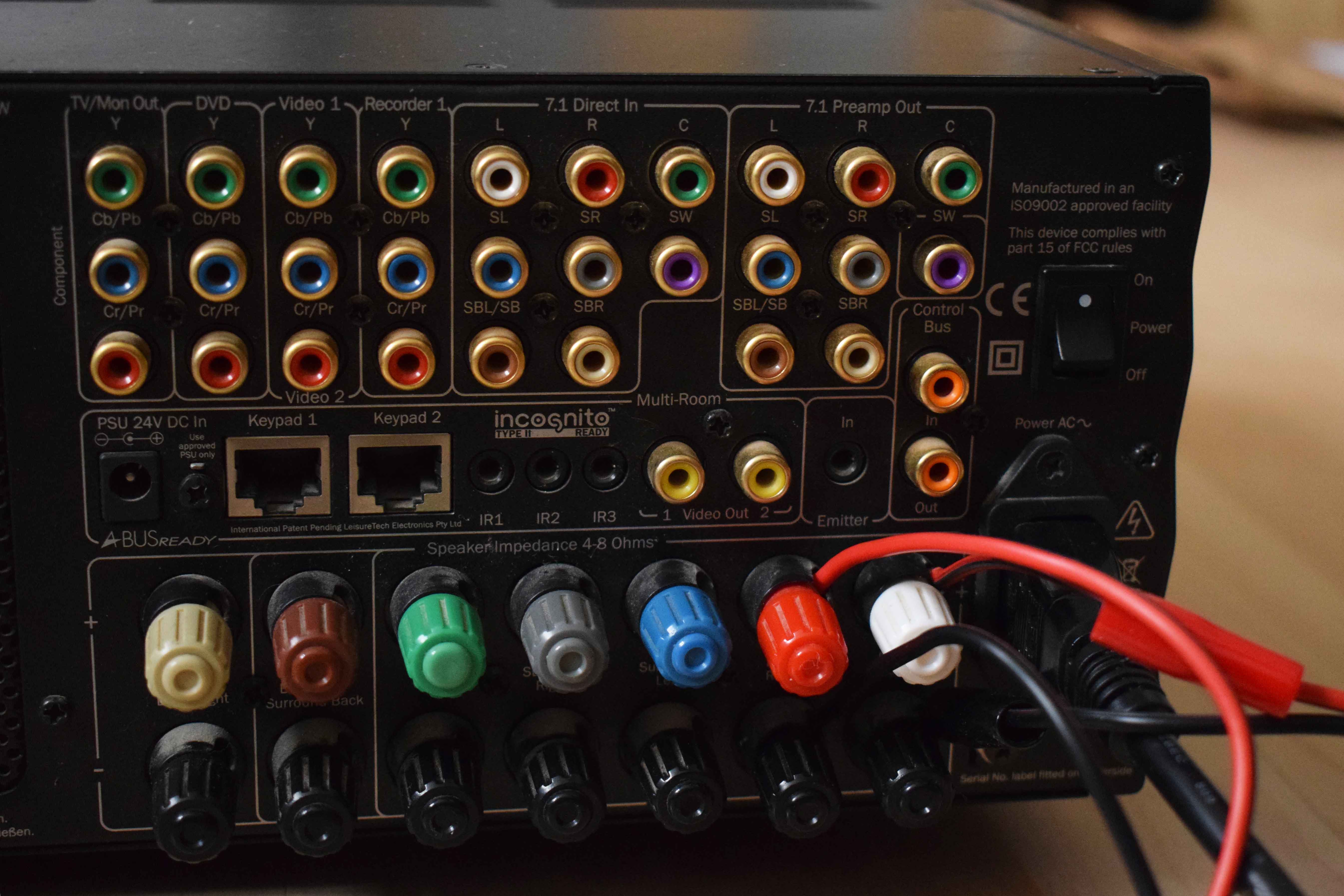
Looking around the back, there are two banks of ports, with a vent in-between. The left side has all the connections to the inputs - Video 1 & 2, Aux, DVD etc - along with its 4 HDMI ports for switching, a serial port, and some antenna ports for the inbuilt tuner. The right side features all speaker connections, component ports, as well as the multi-room ports.
Disassembly & Cleaning
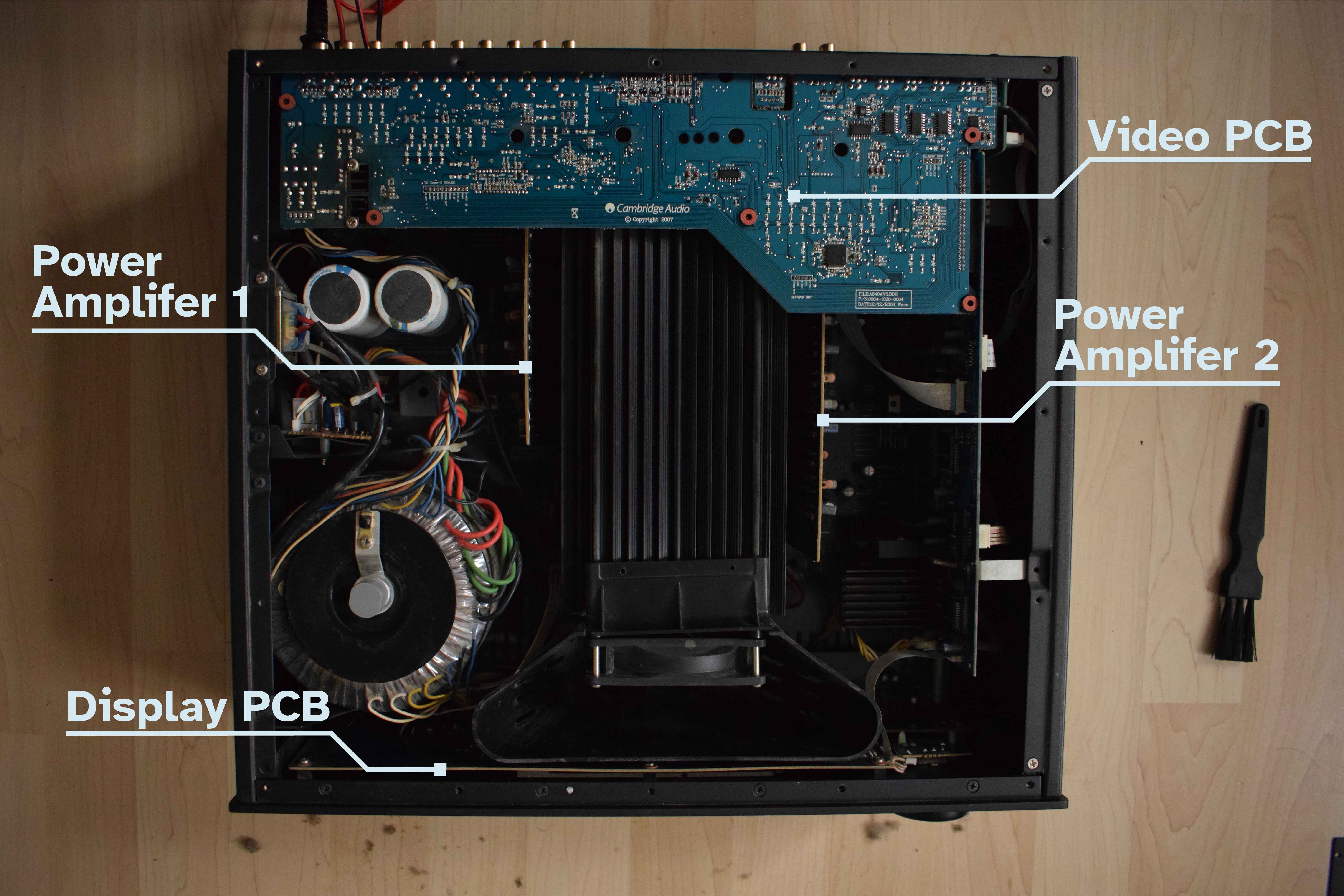
PCB Arrangement
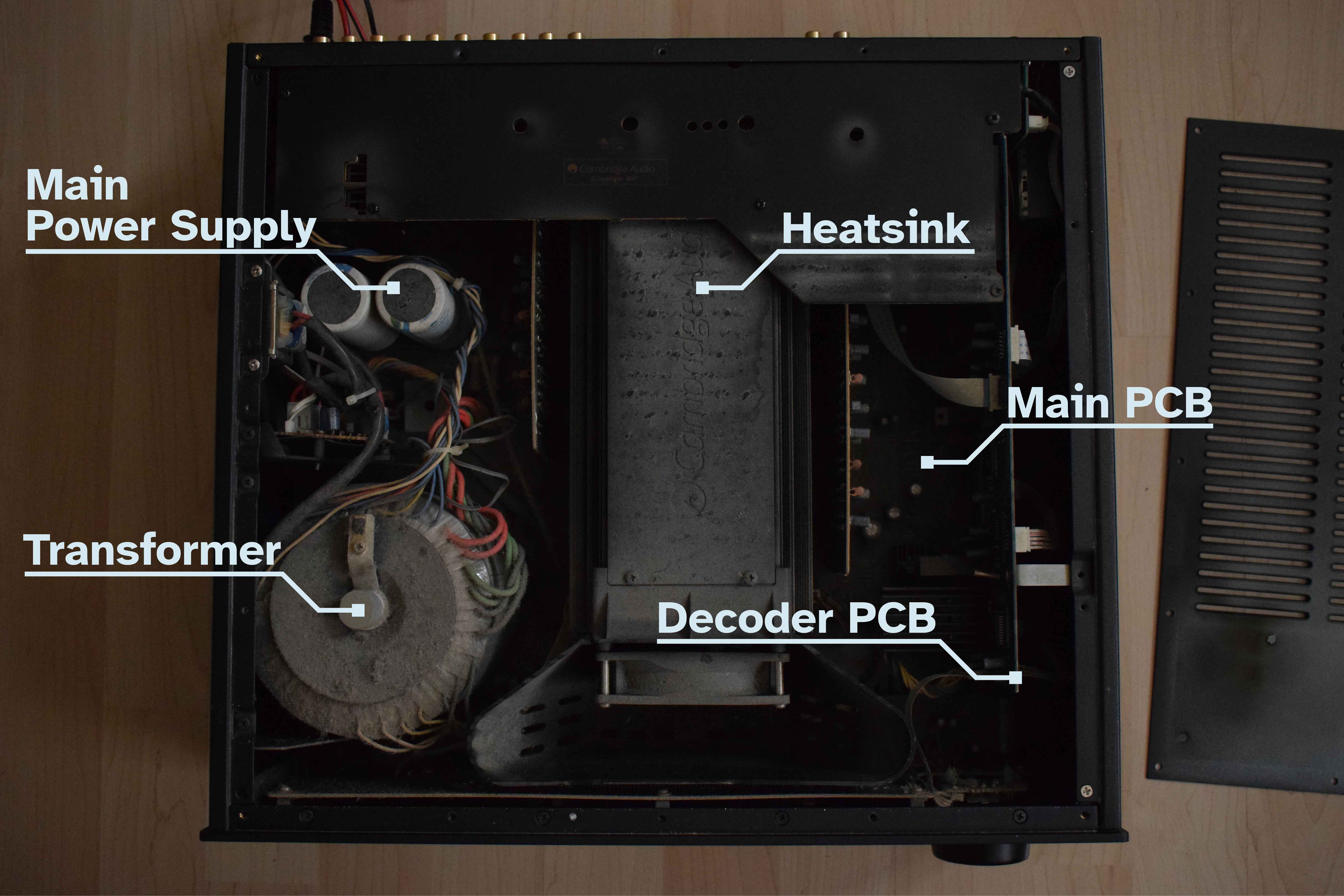
Given its age and vented top, a fair amount of dust has accumulated inside (as well as a concerning amount of wall plaster...), and removing the top cover gives a brilliant view of how all of this works. On the left side is where the power comes in - the large capacitors, some relays, and the giant (and heavy) toroidal transformer. The Main PCB is flat along the bottom of the case, and is basically the size of the case. Three vertical boards connect to this through a many a series of pin headers and screws to secure them in - the inner two are "Power Amplifier 1 & 2" PCBs and are full of resistors, capacitors, transistors, and some diodes; and the rightmost one is the "Decoder PCB". This board features the microcontroller that controls the device, with an on-board power supply for AC to DC conversion (directly connected to the transformer). It features circuitry for digital to analogue converters for all channels, as well as some logic related and some sound processing ICs. In addition, this board then has connections to the tuner, display, and video boards.
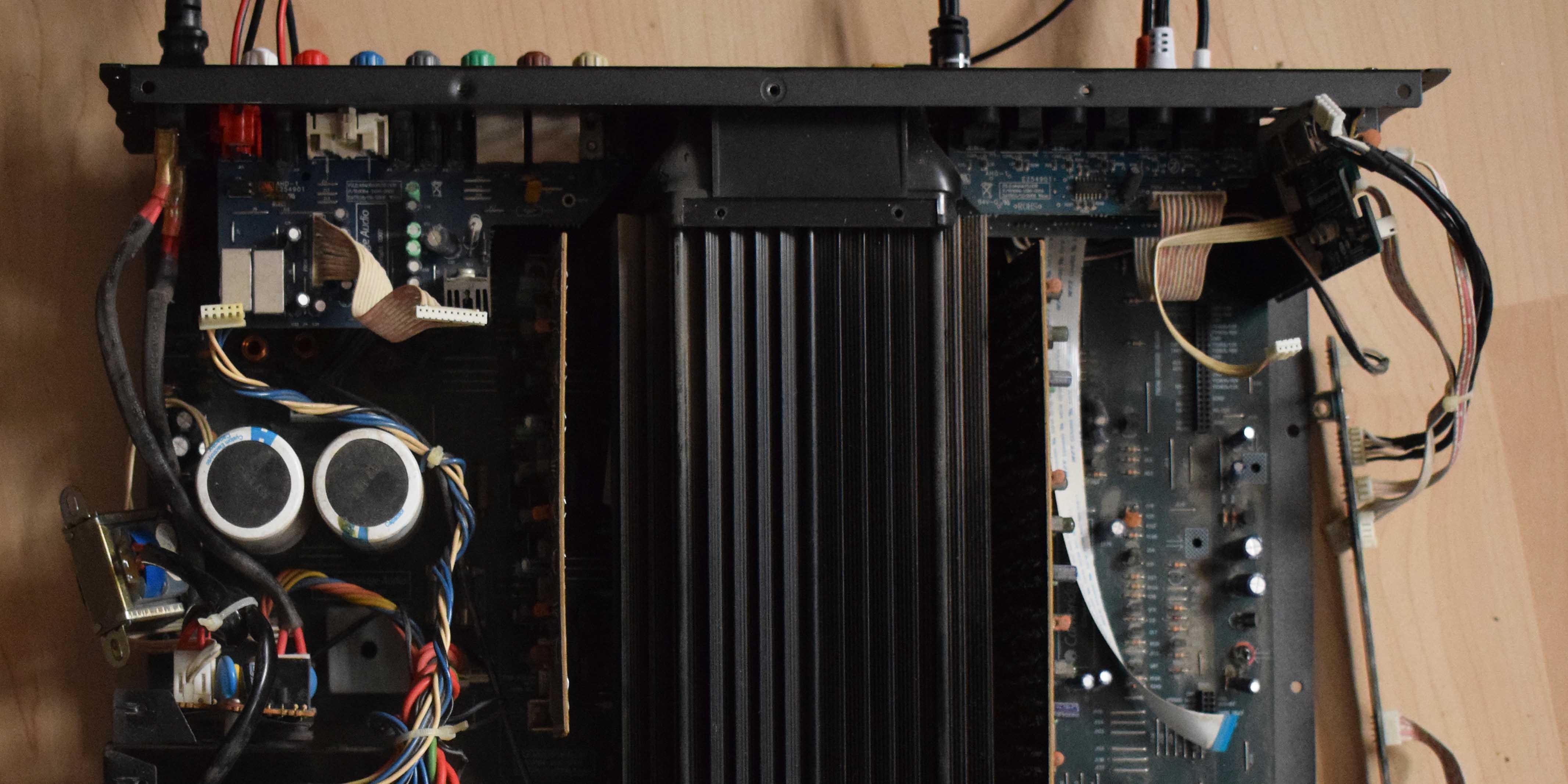
Before cleaning, the internals looked like this:
And after cleaning, it looks a bit better. At the top back, under the plastic sheet, reveals yet another large PCB - the Video board. Here is the display management for the aforementioned HDMI switching, as well as whatever is required for all the digital coaxial, composite, S-Video, and optical S/PDIF TOSLINK connectors to function.
Underneath the Video PCB, you will find that all rear connectors are nested at the back, on a series of perpendicular sub-boards connected to other sub-boards. It's rather interesting how they have utilised the internal space of the amplifier, and I can only really show it through many images once the entire device is mostly disassembled.
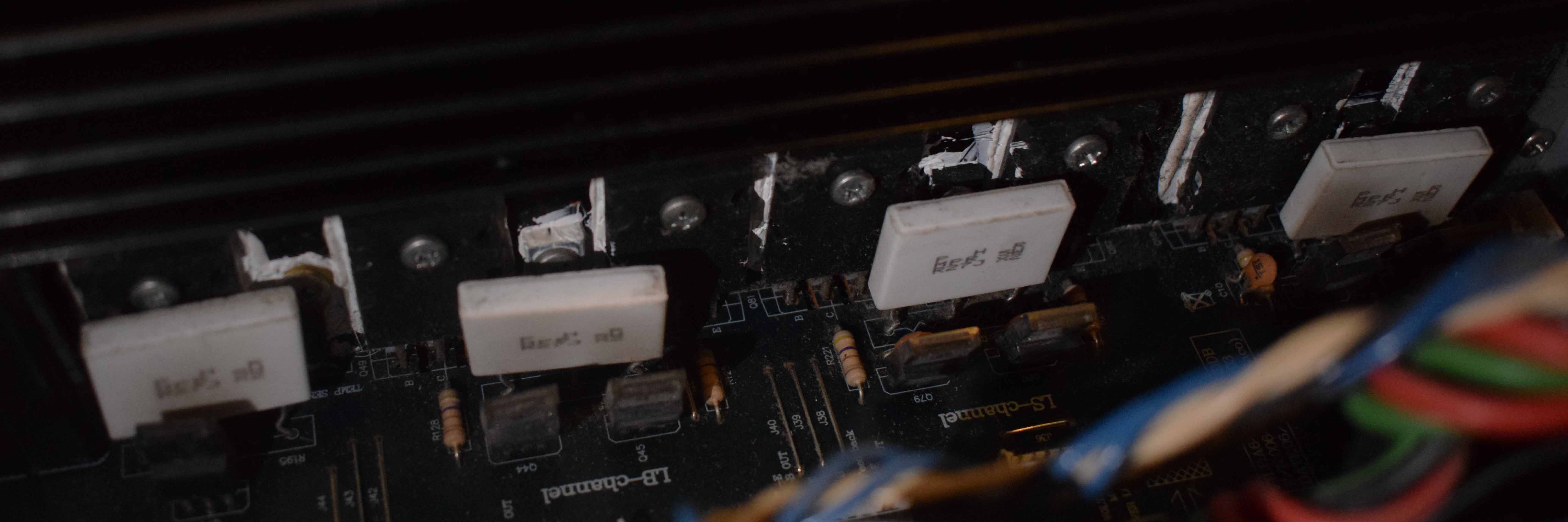
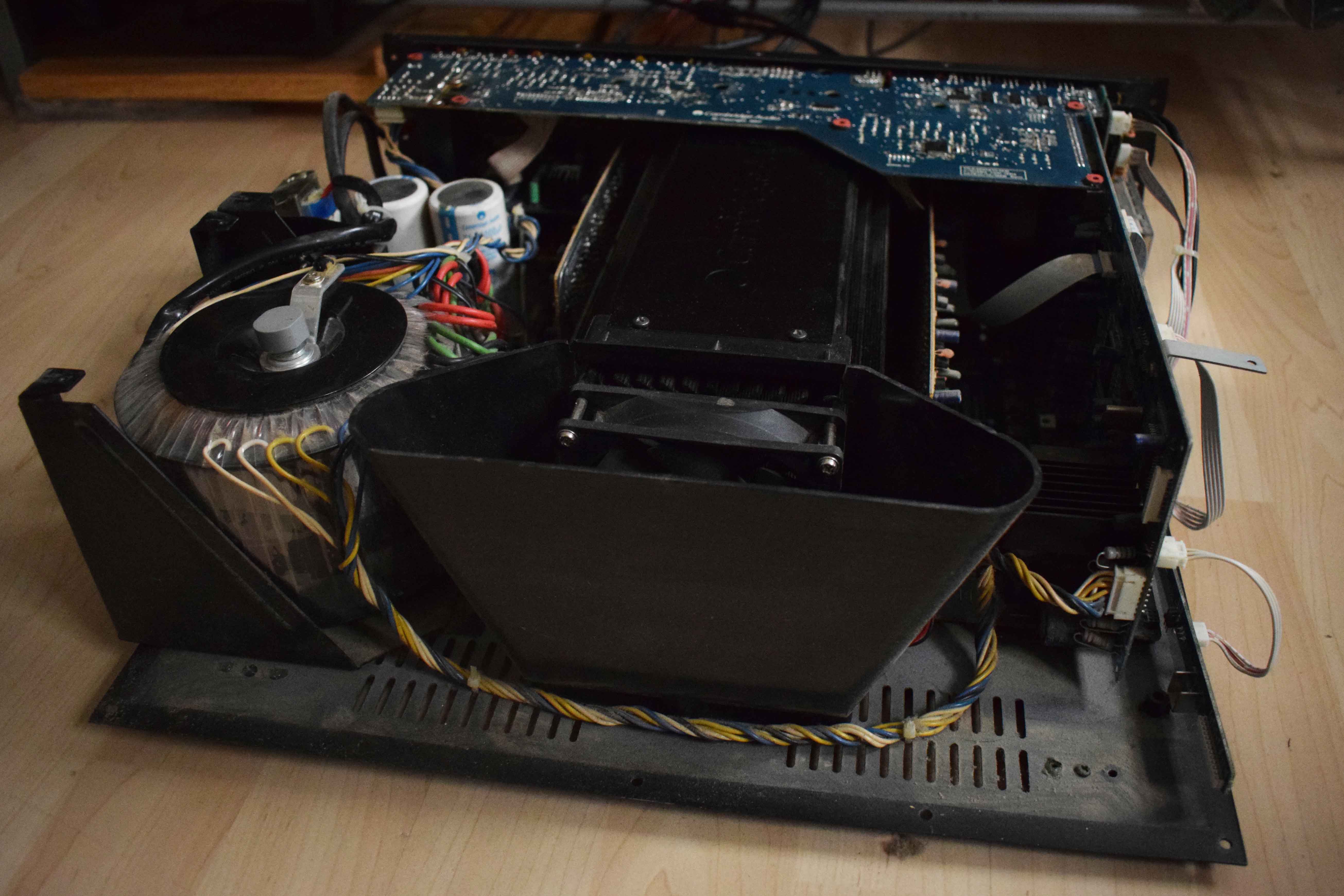
Looking inside, the central rectangle is a massive metal heatsink, with a 90mm fan, that directly connects to the heatsinks of the power transistors (2SA1943) that are rated for 150 watts each.
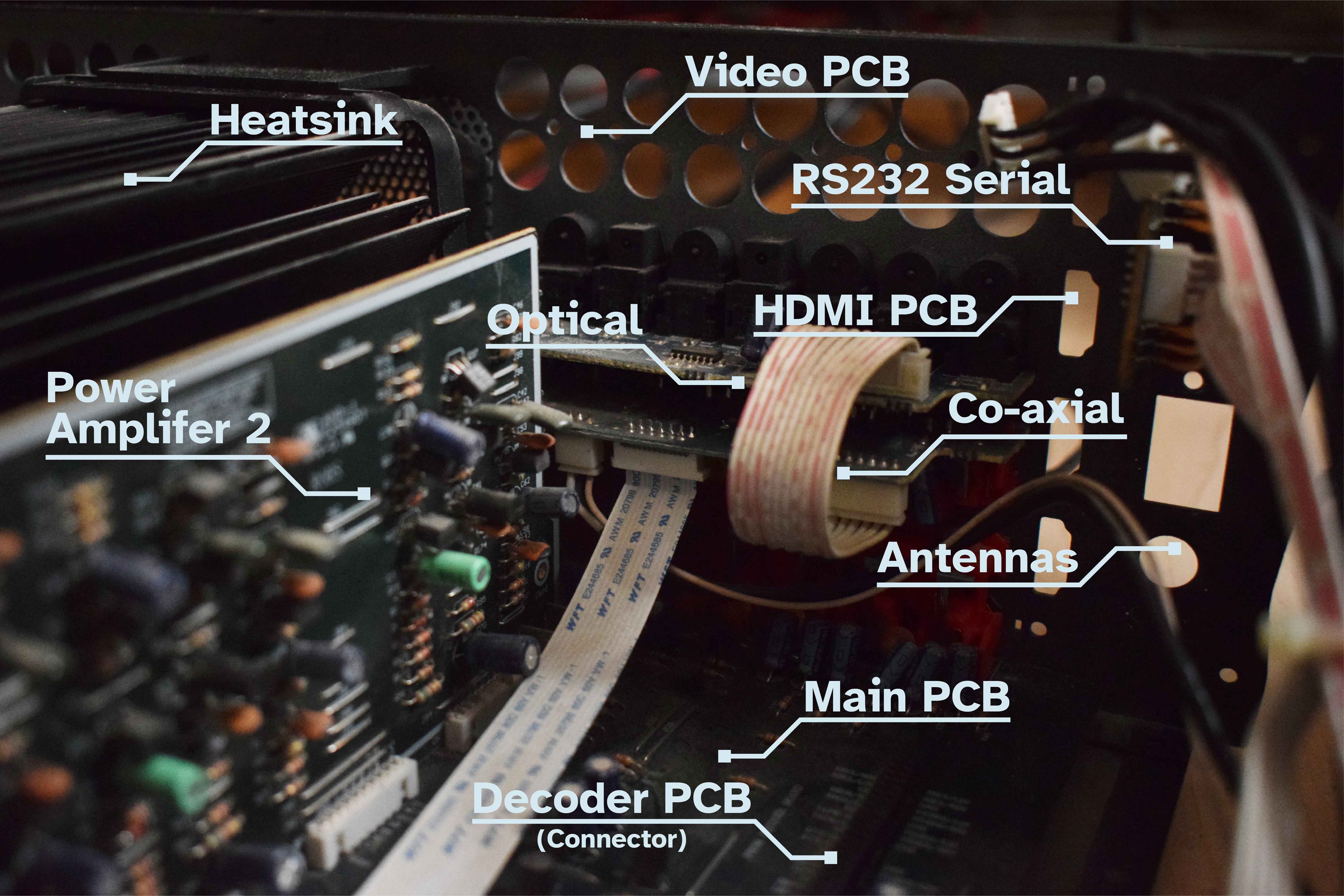
On the right side, with the Decoder and Video PCB removed, the following can be seen: Power Amplifier PCB 2; the Main PCB at the bottom; the connectors for the Decoder PCB; the PCBs for Optical and Co-axial outputs; the places where the HDMI, Antenna and Video PCBs go; and the RS232 connector for serial, shown below.
The left side has the multi-room ports on a horizontal sub-board, and the speaker outputs below are on a vertical board directly behind the speaker protect relays, but this was hard to show.
Case Assembly
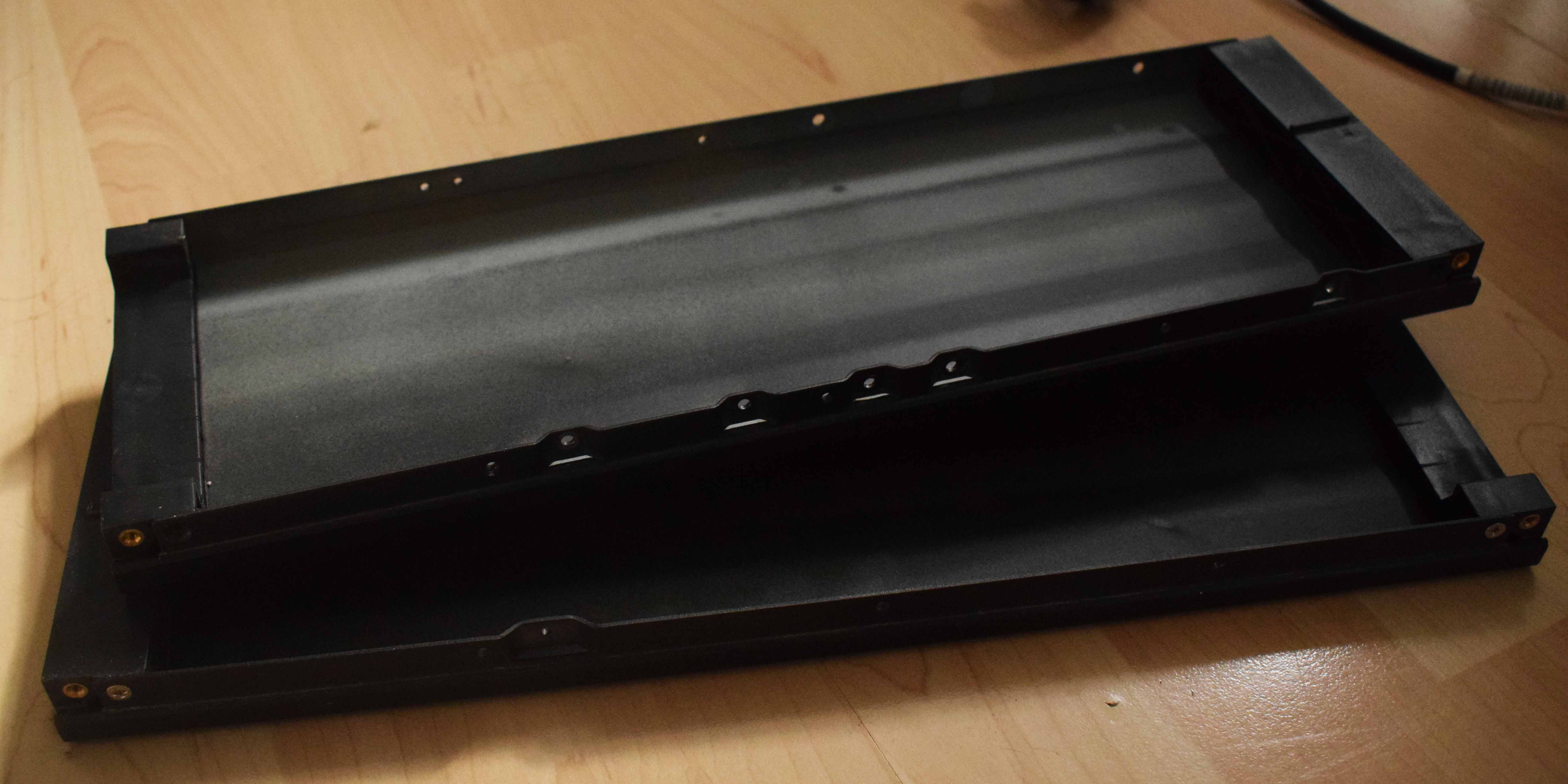
To get to this point, you may have noticed the side panels being removed. These are connected to the top, bottom, and slot in with the front and back panels. They need to be removed before the front assembly, and are shown below - they have a nice zig-zag pattern in them.
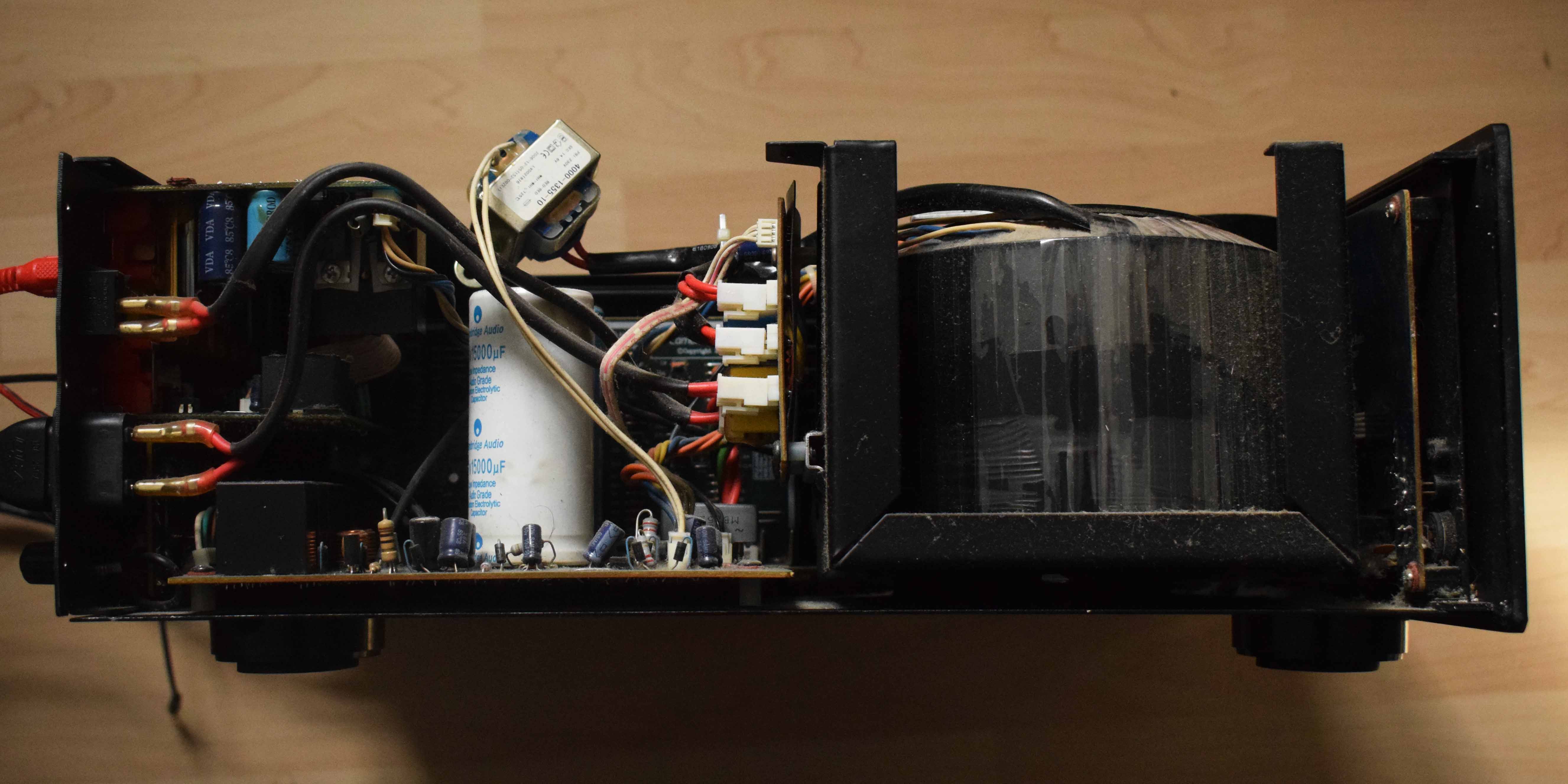
Removing them reveals the side view of the unit, and allowing me access to the power circuitry to inspect the relays and surrounding components (foreshadowing).
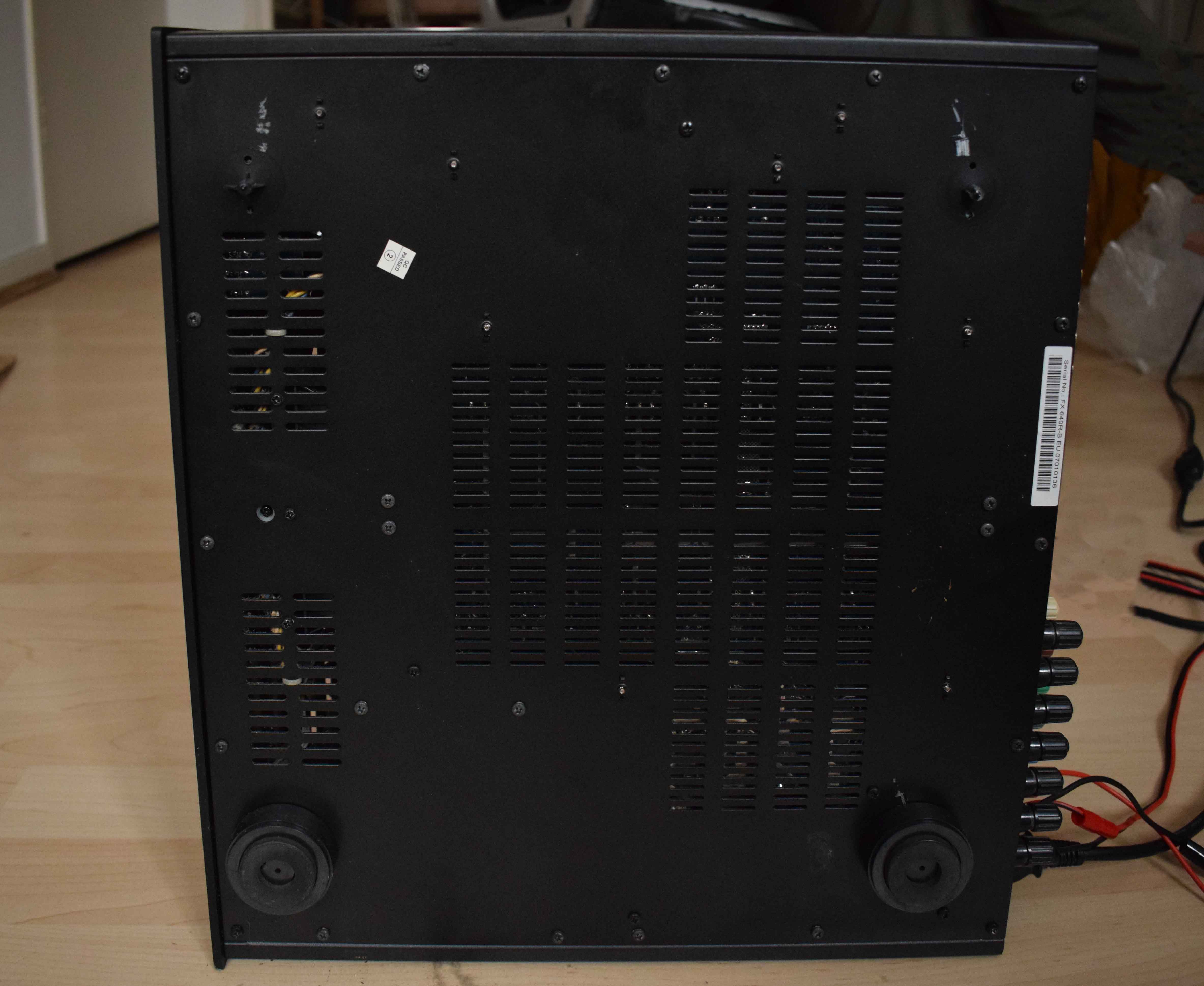
The base of the unit holds most of it together, and mainly has screw points for the Main PCB. You don't really want to remove the back panel as so much more needs to come out and it doesn't serve much purpose. From underneath, it looks like this, with two of the plastic feet missing (that are now just sharp screws scraping across my floor).
To remedy the broken feet, I made a 3D-printable replacements, and the model is available on Thangs, if you were in need. To be able to replace them, it does have to be fully disassembled though.
With all the PCBs and non of the panels, this is what it looks like:
But lets take a closer look at everything inside...
PCBs
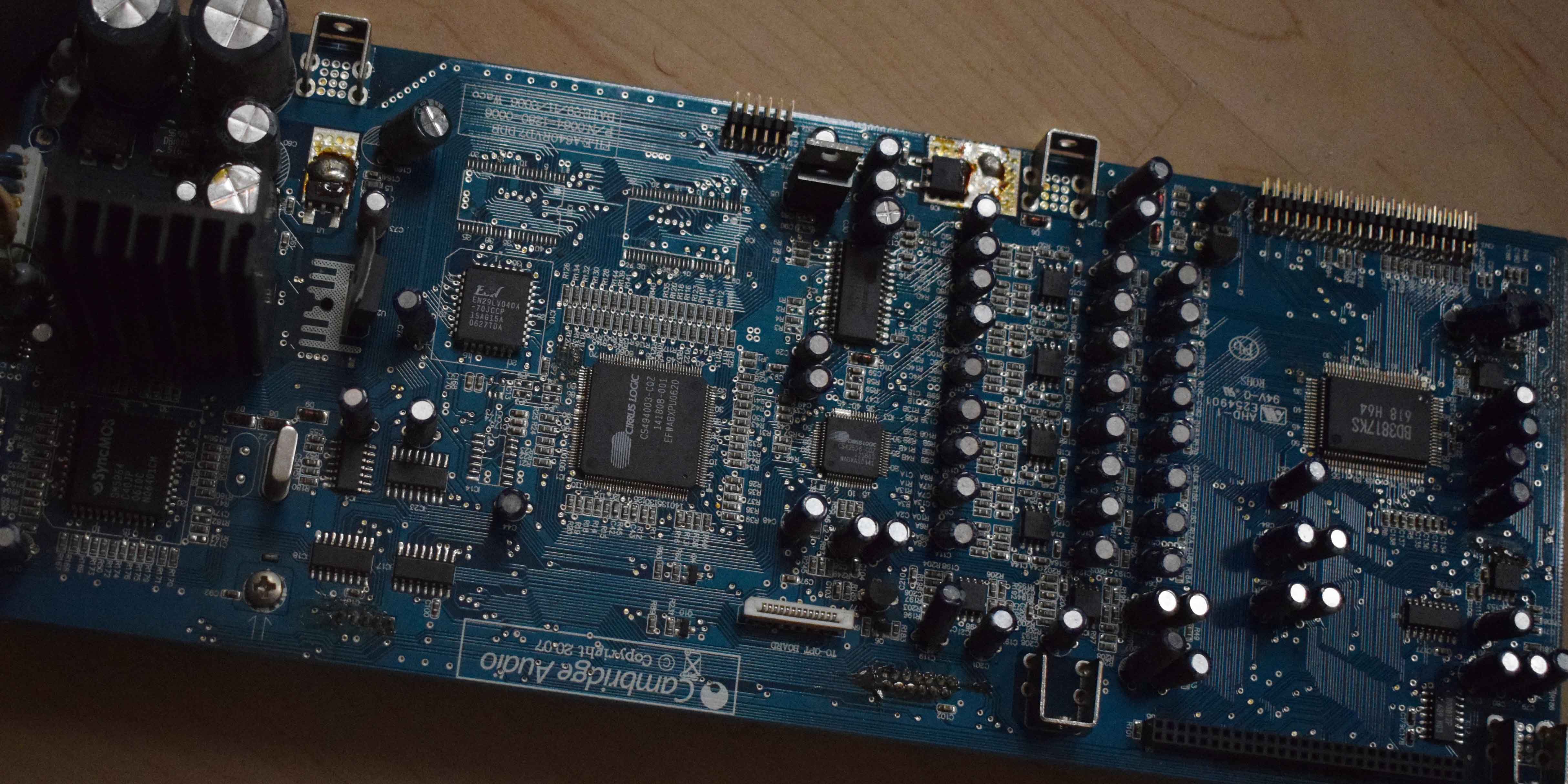
The Decoder board is the star of the show, with all the interesting electronics - and there's plenty of it. The large Cirrus Logic IC in the middle (CS494003-CQ) is a "Multi-Standard Audio Decoder and Programmable Digital Signal Processor". Then to the right, you will find a CS42526-CQ which is a 6-channel CODEC with S/PDIF Receiver. Above this one is a 28L SOIC package which I believe to be a CS43122 122dB 24-Bit 192kHz DAC. In addition, there is an EON EN29LV040A 4Mb CMOS Flash module supporting a SyncMOS SM5964C40J 8-bit microcontroller. And, on the right end of the image, is a BD3817KS providing 7-channel volume control.
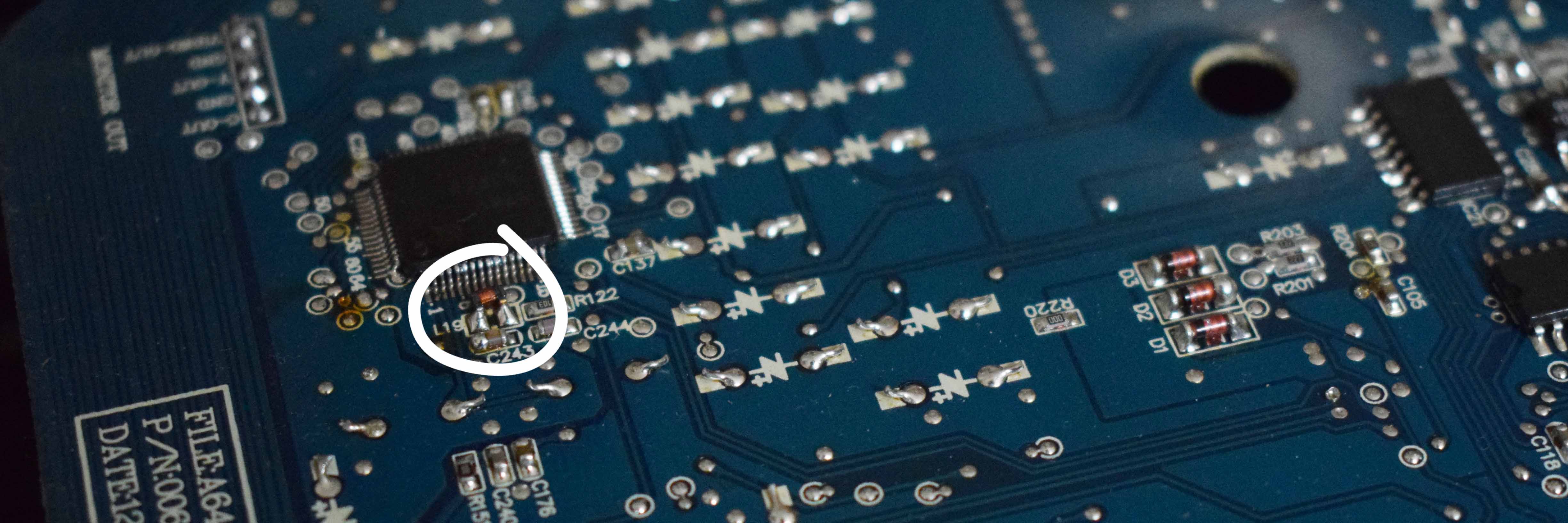
I'm yet to test the functionality of the video, HDMI, and coaxial boards, as whilst I'm sure it would be useful, I haven't had the time. Either way, there are a number of darker patches (like burn marks) around this board, but what jumped out at me (literally) was this inductor on the Video PCB. The only reason I can think of to explain this level of attachment is that something got too hot and melted the solder, but I honestly have no idea.
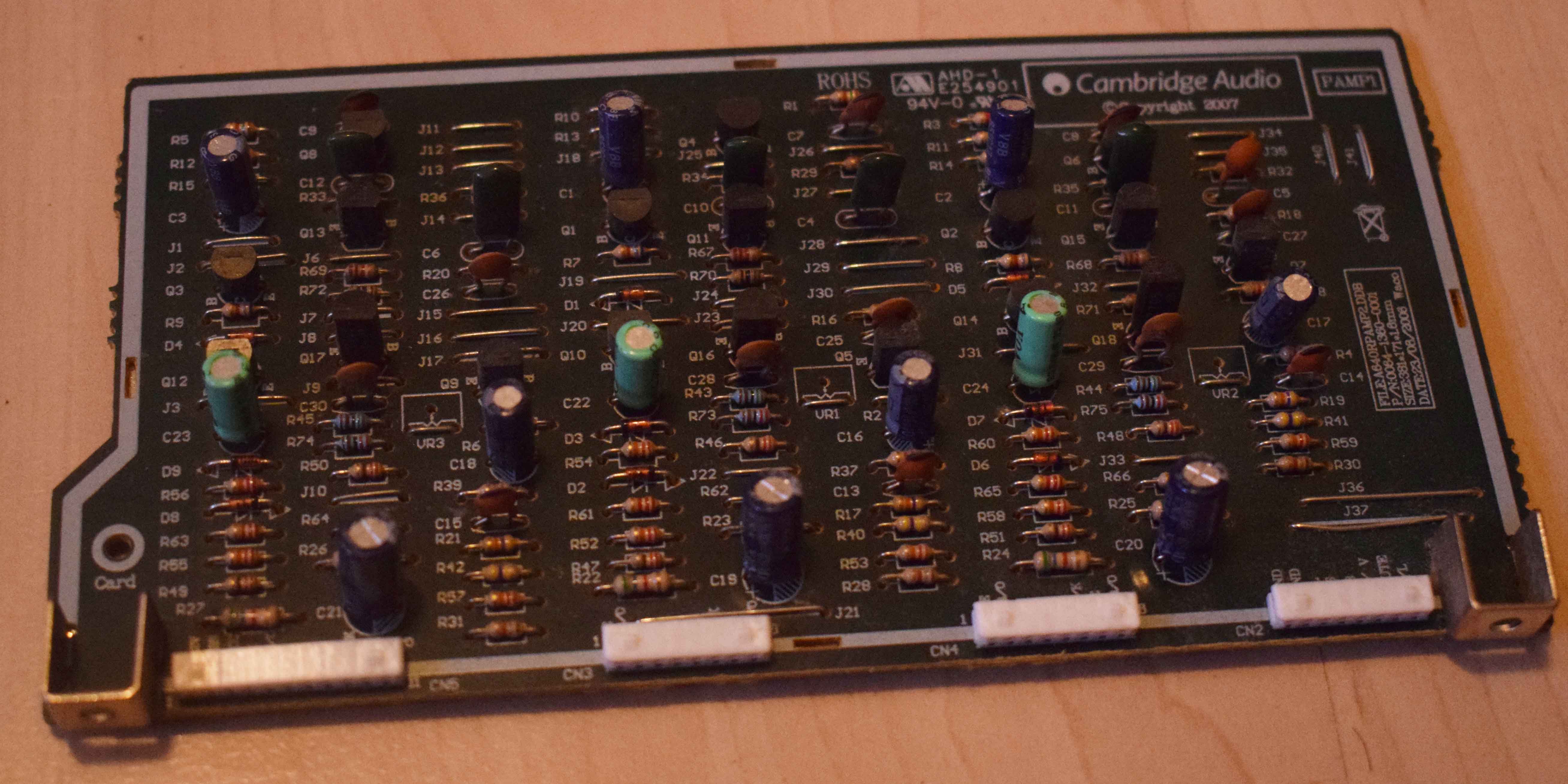
The power amplifier boards, I find kind of amusing - they just contain mostly passive components, nicely arranged, with headers to connect to the mainboards. They're all through-hole components and there's not much more than that. I'm assuming it was done like this for cost related reasons.
There are many more boards, and a lovely exploded diagram can be found in the service manual, but I don't want to bore you with my ramblings, so lets move on.
Front Display Assembly
The last part to look at in detail is the front display module. By the time I got around to disassembling this, the light had gone outside, so please excuse the orange kitchen lighting.
This piece is rather heavy; everything is mounted to a thick metal sheet that makes the front of the device. The construction is also rather interesting - on the other side it has perpendicular rails with screw holes, which allow it to be connected to the side pieces of the chassis and creates the structure of the box. But within these rails, it has a thin inner frame of which the PCB mounts to, the buttons sit on, and the volume potentiometer screws into. This is shown below and I'm not quite sure why this was done. As far as I can tell, it mostly just offset the PCB from the front plate, which is was probably necessary for the screen.
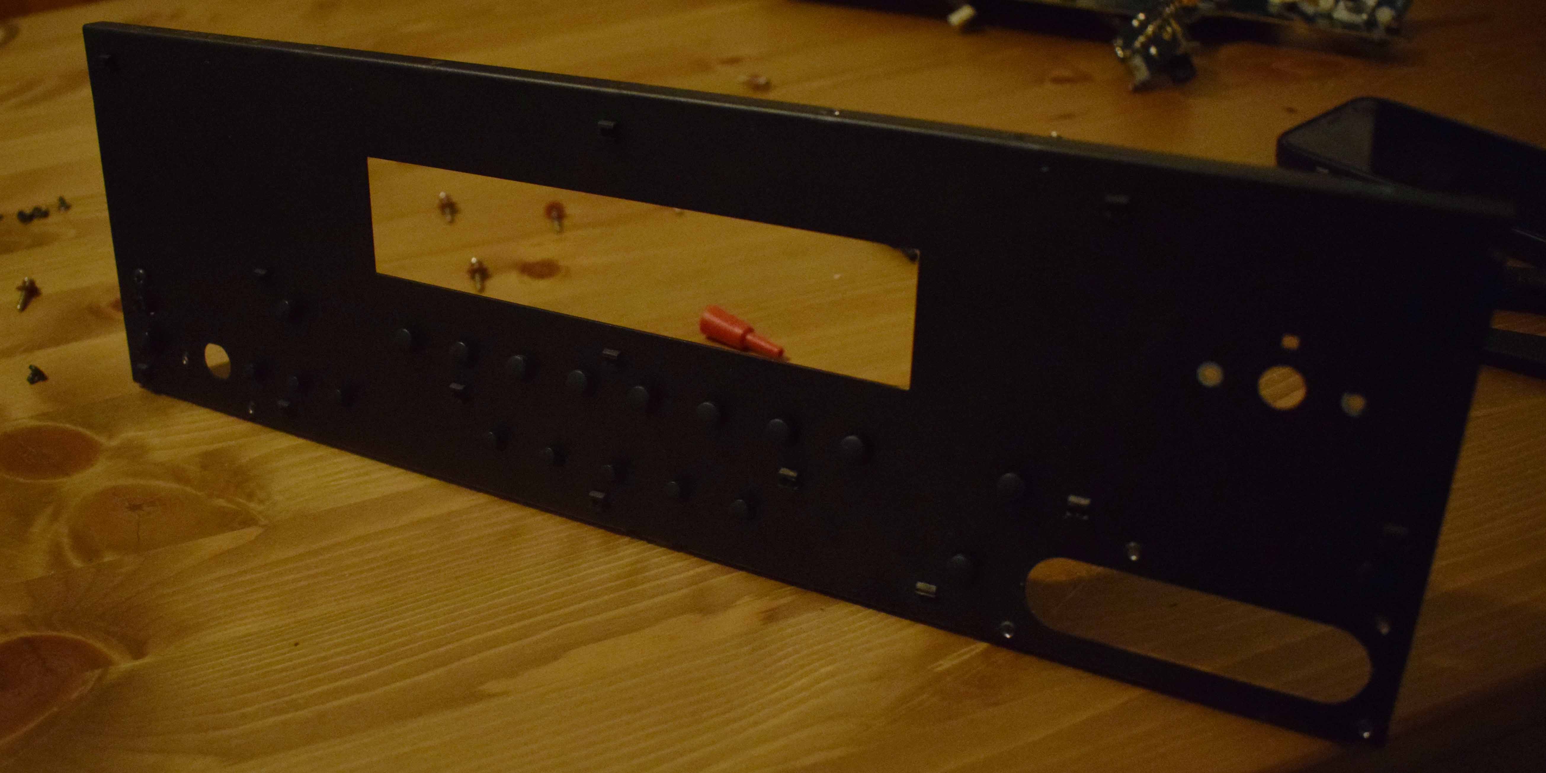
Regarding the "Video 3" connectors which are hidden under a removable cover, there is an addition piece that clips into the front frame that forms the back wall of these ports. To finish it off, there is also a lens over the display (that was absolutely filthy) which is glued to the front.
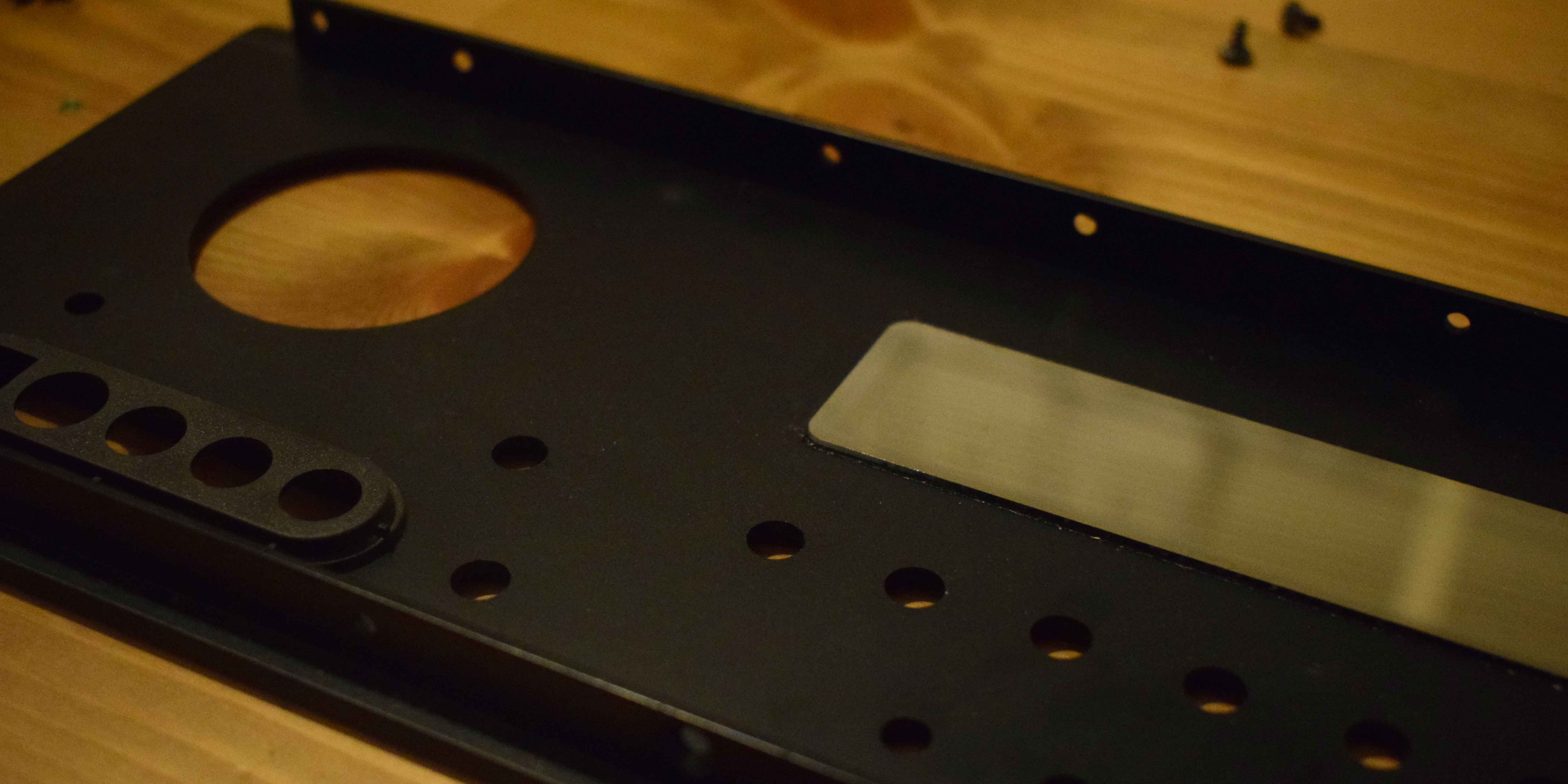
it is also apparent the volume potentiometer has been bonked at some point (probably in shipping), and has warped the inner frame - this metal is meant to be flat and parallel with the front:
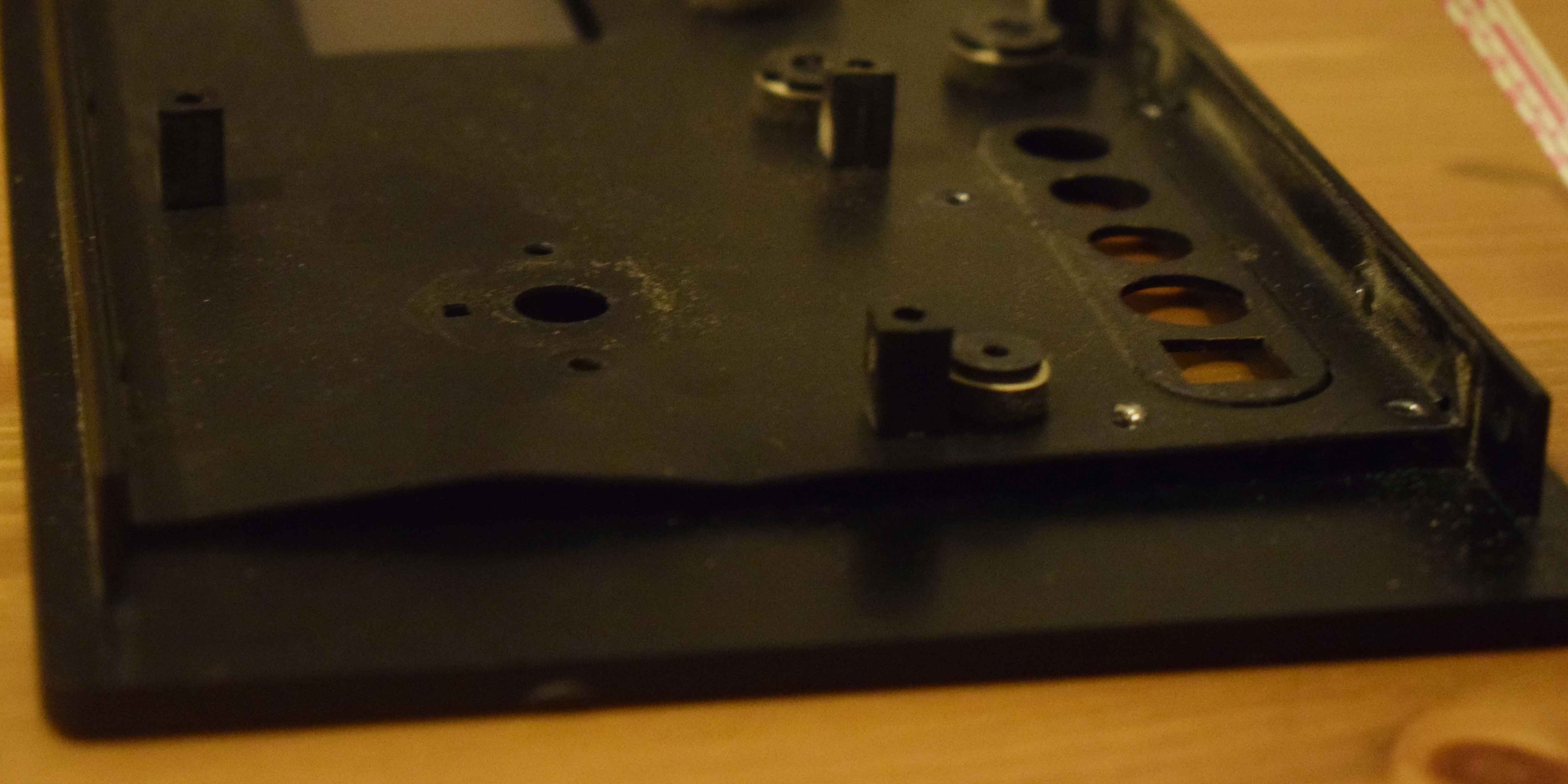
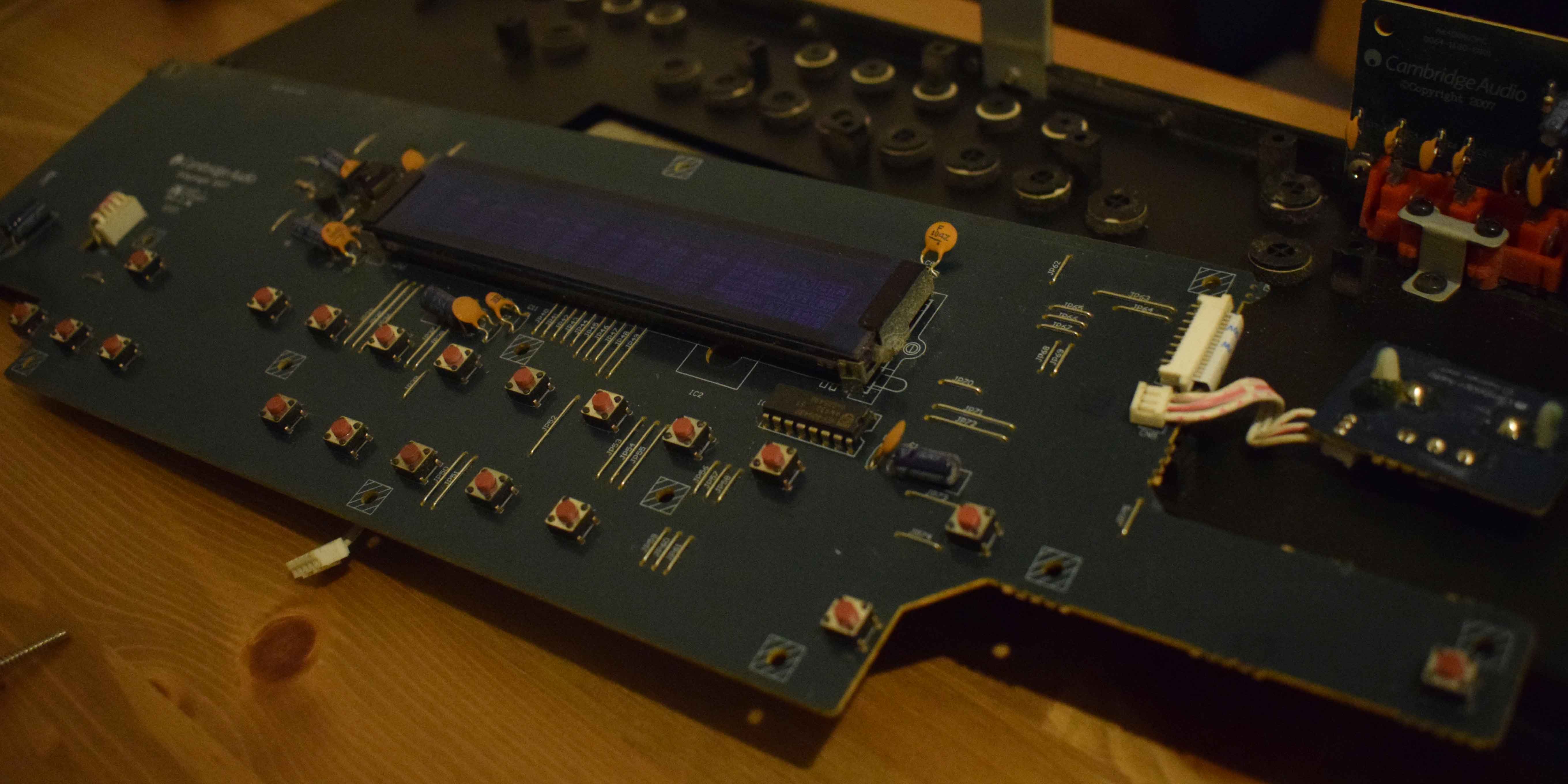
As mentioned, the Display PCB is mounted to the inner frame of this, which is where the VFD is featured in all of its glory. This board is unsurprisingly quite empty as it is just a series of buttons and the display. The potentiometer is on the small rectangular board to the right and is connected to the Display PCB. Then the Display PCB connects to the Main PCB, via a 5-pin connector. The phones output has its own 4-pin connector to the Main PCB, and the Video 3 connectors go via a long slim PCB which eventually connects back to the Decoder PCB. This whole assembly was a pain to get apart...
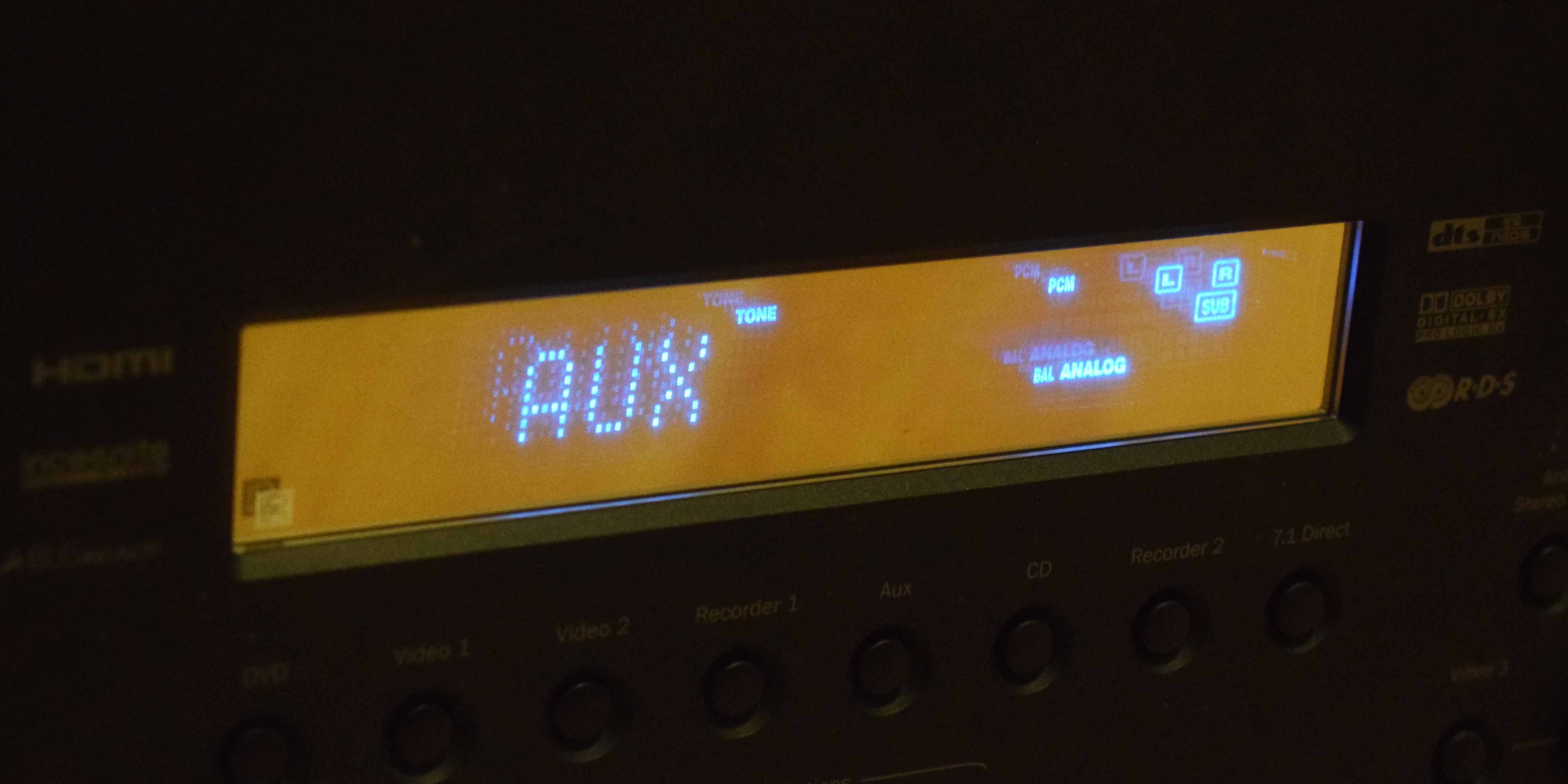
...but at least it achieved something - cleaning the display lens. They aren't quite comparable but here are images from before and after. It was notably brighter after, and looks significantly better.
Power & Relays
I paid surprisingly little for this, and whilst it works, it has a hissy fit every time it turns on. In the power section at the back left corner, a bank of 4 relays sit together quietly and patiently waiting for power - and once they receive it they make it known to the whole room. Louder than I would normally listen, the relays constantly click on and off for a variable duration of time. Although normally for around 20-30 seconds, it can occasionally be a few minutes before it's quiet. Once it stops, everything works perfectly.
These are the speaker protect relays, and given its age, it's a fairly normal point of (partial) failure. Given they are switching, it likely means that this issue isn't caused by defective relays, but something wrong with the surrounding circuitry - particularly old or degrading capacitors. Whilst it took me a fair while to diagnose the issue with a multimeter, half an hour with an oscilloscope made it obvious. The main problem is that it's quite hard to probe the Main PCB whilst it is powered on, and if you want to replace any components, you have to take everything apart to access the underside of the Main PCB.
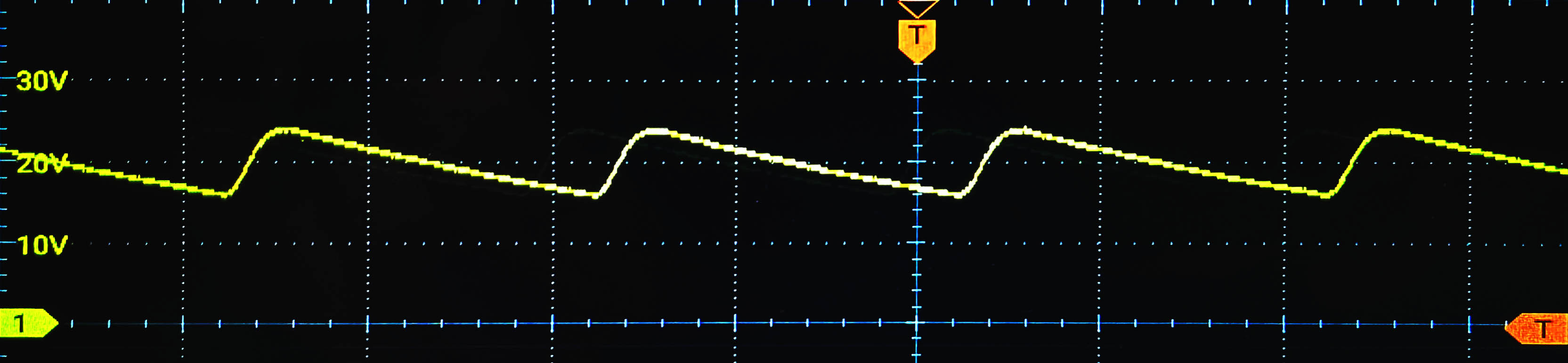
Diving in to the service manual, reveals the importance of two main things - the Decoder PCB and its "Protect 1" and "Protect 2" signals which come directly from the main processor, and the relay supply. In my case, the issue was with the latter, and in particular "C96". As designated in the service manual, C96 is a 470uF 25V rated capacitor which is designed to smooth the rectified output voltage from the transformer. Given it uses a half-wave rectifier, and C96 barely charged (or at least not quickly), the supply voltage for the relays varied between 0-24V 50 times per second. Hence, this rapidly turned on and off the relays as the coil was not sufficiently powered.
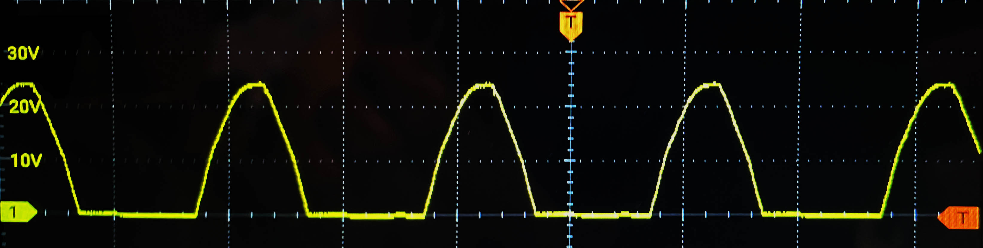
Eventually, the capacitor would charge (just about enough), such that it varied between 4-24V, and was able to keep the coil engaged at all times.
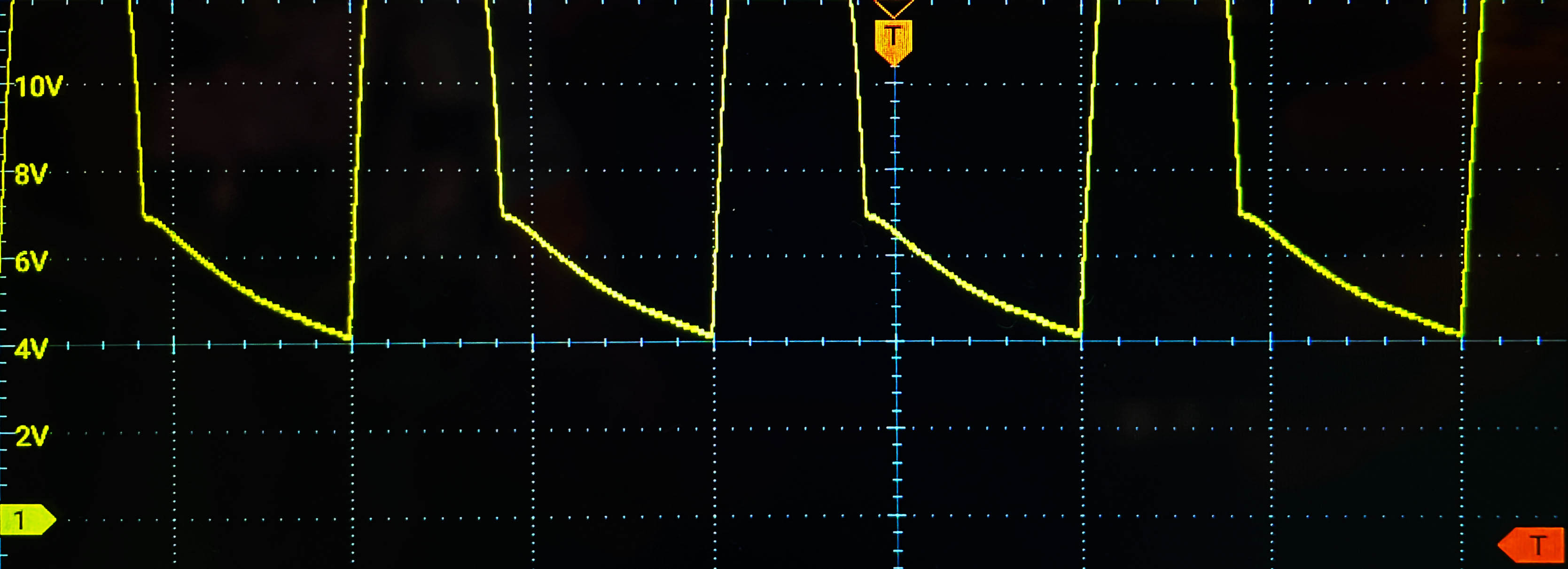
So lets fix it! Its as simple as replacing the capacitor, and now the voltage ripple is contained between 14-24V.
Closing Thoughts
You've made it to the end, so now you get to know the grand sum that I coughed up for this amplifier. I spent a total of £27.19, including postage. It didn't come with a remote, made horrific sounds when turning on, and was missing two feet, but it certainly powers speakers. I think I got a decent deal on this one regardless. It's probably worth its weight in metal alone...